Samsung Bets $73 Billion to Dethrone SK Hynix as Nvidia's AI Memory King
Samsung Electronics just committed to spending $73 billion on AI chip infrastructure in 2026 - a 22 percent jump from last year that signals something has gone deeply wrong inside the world's largest semiconductor company, and that it intends to fix it with a mountain of cash.

The announcement, made by Samsung co-CEO Jun Young-hyun and confirmed Wednesday, is about more than chips. It's a multi-billion-dollar admission that Samsung lost the memory wars - for now - and a declaration that it won't stay lost.
The specific target: SK Hynix, Samsung's South Korean rival, which has quietly seized dominance in High Bandwidth Memory (HBM) - the specialized chips that sit inside Nvidia's AI accelerators and do the heavy lifting for large language models, image generation, and the entire modern AI stack.
$73 billion is not a number you commit to lightly. For context, that's roughly the GDP of Morocco, or more than three times what Intel spent on capital expenditure in all of 2024. Samsung is essentially betting its next decade on one outcome: that AI demand will remain voracious, and that whoever wins the HBM race wins the AI era.
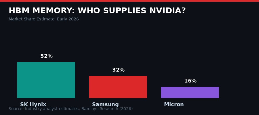
HBM market share breakdown, early 2026. Source: Industry analyst estimates, Barclays Research.
How Samsung Lost the HBM Race

Advanced semiconductor packaging is where Samsung fell behind - and where the $73B is aimed.
The HBM story is one of the stranger reversals in tech history. For most of the past three decades, Samsung was the undisputed king of DRAM - the type of memory chip that HBM is derived from. Samsung invented 1Gb DRAM in 1996. It built the largest memory fabrication footprint on the planet. It outspent every competitor and usually won.
Then Nvidia's AI accelerator business exploded, and the game changed.
HBM is not ordinary DRAM. It requires stacking memory dies on top of each other using a technology called through-silicon vias (TSVs) and then connecting them to a logic processor using advanced packaging called 2.5D interposers or CoWoS (Chip on Wafer on Substrate, in the TSMC terminology). Getting this right requires precision at a scale that most fabs weren't designed for.
SK Hynix, smaller than Samsung and historically the number two player in memory, made a strategic call around 2020 to prioritize HBM development. They poured resources into HBM2E and then HBM3 qualification, specifically targeting Nvidia. When Nvidia's H100 became the most coveted chip in human history following the ChatGPT boom, SK Hynix was already Nvidia's primary HBM supplier.
Samsung, meanwhile, was running into qualification problems. Reports from late 2024 and early 2025 indicated that Samsung's HBM3E chips were generating more heat than Nvidia's thermal specs allowed, failing qualification testing repeatedly. Nvidia reportedly continued using SK Hynix as its primary supplier while keeping Samsung on a reduced allocation.
"Samsung's memory division posted its worst quarterly performance in years in late 2024. The company's traditionally impenetrable market position in DRAM was being eroded by a competitor it had always outspent. The HBM failure wasn't just a product problem - it was an identity crisis." - Industry analyst commentary, Reuters, January 2025
By early 2026, the market picture looked bleak for Samsung. SK Hynix held an estimated 52 percent of the HBM market. Samsung sat at around 32 percent, having recovered somewhat with HBM3E product improvements and the beginning of HBM4 sampling. Micron, the American memory giant, had grown its slice to roughly 16 percent with aggressive US government tailwinds and strong HBM3E yield rates.
The $73 Billion Plan: What's Actually Being Built

Advanced semiconductor fabs require billions in capital to build and equip. Samsung's spending jump targets the packaging and HBM layers.
When Samsung's co-CEO Jun Young-hyun said that "demand for agentic AI is fueling a surge in orders," with funds going toward "future-oriented" sectors like advanced robotics, he was speaking in the carefully calibrated language of a company that has already decided where the money goes. The $73 billion doesn't land evenly across Samsung's vast business empire.
Three areas are absorbing the bulk of the investment, based on Samsung investor briefings and analyst breakdowns:
HBM4 and next-generation memory R&D is receiving the largest share - estimated at roughly 34 percent of the total. Samsung is pushing to mass-produce HBM4 at competitive yields before SK Hynix locks up the next generation of Nvidia contracts. HBM4 offers approximately 50 percent greater bandwidth than HBM3E, using a 12-high stack architecture with tighter tolerances on thermal management. Getting Samsung's HBM4 through Nvidia's qualification process is the single most important milestone in this entire plan.
Foundry expansion and advanced process node scaling absorbs roughly 22 percent. Samsung's foundry division - which competes directly with TSMC for fabbing third-party chips - has been losing customers for years. Apple moved fully to TSMC. Qualcomm shifted major Snapdragon orders. TSMC's yield rates on 3nm and 2nm nodes have consistently outperformed Samsung's. The company is spending heavily to close this gap, with reports of significant capacity expansion at its Pyeongtaek complex in Gyeonggi Province, South Korea's largest fab site.
Advanced packaging is getting around 15 percent of the budget. This is arguably the most critical investment category, because advanced packaging is where Samsung's HBM failed in the first place. CoWoS-equivalent technology, through-silicon via quality, and the thermal management systems that surround memory stacks are all in this bucket. Samsung has been building out its own Interconnect Technology Lab infrastructure, competing with TSMC's CoWoS dominance.
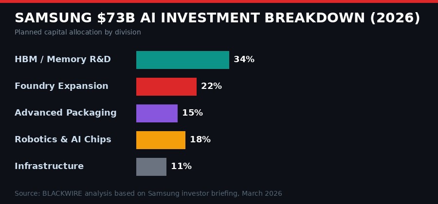
Estimated allocation of Samsung's 2026 AI capital budget. Source: BLACKWIRE analysis based on Samsung investor briefing, March 2026.
The remaining capital flows into robotics and AI chip design (18 percent) and general infrastructure (11 percent). The robotics allocation is notable - it signals Samsung's intent to be a physical AI player as well as a component supplier, matching a trend set by Nvidia at GTC 2026 where Jensen Huang spent significant keynote time on humanoid robots, autonomous vehicles, and physical AI systems.
The Nvidia Factor: Why HBM Is Everything

The AI chip stack is now the most strategically valuable product in the semiconductor industry.
To understand why Samsung is willing to spend $73 billion chasing HBM market share, you have to understand what HBM means in the AI supply chain.
Every Nvidia H100 contains six HBM3 stacks providing 80 GB of memory and 3.35 terabytes per second of memory bandwidth. The upcoming B200 Blackwell chips use HBM3E and push bandwidth even higher. Nvidia's GB200 Grace Blackwell Superchip - the system-level product being deployed in most hyperscaler AI factories right now - uses HBM3E at 8 TB/s aggregate bandwidth per rack-scale system.
At Nvidia's current revenue trajectory - Jensen Huang projected "at least $1 trillion in revenue from 2025 through 2027" at GTC 2026 - the HBM content per Nvidia chip represents somewhere between 30 and 40 percent of total system cost. That makes HBM one of the highest-value components in the most valuable computing platform ever built.
Whoever supplies that HBM prints money. SK Hynix's HBM sales have been the primary driver of its turnaround from a company once considered a potential acquisition target to one of the most profitable semiconductor firms in the world. In 2024, SK Hynix's operating profit surpassed Samsung's semiconductor division for the first time ever - an event that, inside Samsung's headquarters in Suwon, landed like a thunderbolt.
"The company is increasing production and research investments by 22 percent in 2026 in an attempt to overtake SK Hynix's lead as Nvidia's dominant memory provider. Co-CEO Jun Young-hyun says demand for agentic AI is fueling a surge in orders." - The Verge, March 19, 2026
The competitive geometry is getting more complicated, however. Nvidia is not a passive participant in the memory wars. It has strong incentives to maintain multi-supplier HBM sourcing. A supply chain dependent on a single provider - even a reliable one like SK Hynix - creates leverage that chip suppliers can eventually use to negotiate higher prices. Nvidia has been actively working to qualify Samsung's HBM products and to grow Micron's share, precisely to maintain bargaining power.
This means Samsung doesn't need to beat SK Hynix outright. It needs to qualify well enough that Nvidia allocates a larger portion of its orders - even 40 percent would represent billions in additional annual revenue and would validate the $73B investment thesis.
The HBM4 Qualification Race

HBM4 production requires precision stacking of up to 12 memory dies with micron-scale tolerances.
The battleground that will determine whether Samsung's $73B bet pays off is HBM4 qualification.
HBM4 is the next generation of AI memory, designed to meet the bandwidth demands of Nvidia's post-Blackwell architectures - the Vera Rubin generation that Huang announced at GTC 2026, slated for delivery in 2026 and 2027. It uses a base die logic layer manufactured at a leading-edge process node (5nm class), stacked beneath 12 DRAM dies using through-silicon vias, reaching a total stack height of roughly 720 microns.
The thermal challenge is the hardest part. AI training and inference workloads push memory chips to sustained high temperatures. HBM's stacked architecture concentrates heat in a small physical space. The failures Samsung experienced with HBM3E were primarily thermal - chips that ran hot enough to exceed Nvidia's operating limits and cause signal integrity issues at high frequency.
Samsung says it has addressed these issues. Industry reports from January 2026 indicated Samsung's HBM3E yield rates had improved significantly, crossing Nvidia's qualification thresholds for at least some product configurations. HBM4 prototypes were reportedly sampling to Nvidia in Q4 2025, with full qualification testing expected through the first half of 2026.
SK Hynix is not standing still. It publicly committed to HBM4 mass production in 2026 and has been expanding its M16 fab in Icheon for this purpose. The race is genuinely competitive - and the margin is narrower than it looked a year ago, when Samsung's thermal problems seemed intractable.
What "qualification" actually means: When chip companies talk about qualifying a supplier, they mean running extensive testing of that supplier's components in real system conditions - running AI workloads, stressing thermal limits, checking signal integrity at high frequencies, and verifying long-term reliability. For HBM, Nvidia's qualification process reportedly takes 6-12 months and requires consistent yields above 80-90 percent for production allocation. Samsung cleared a version of this bar for HBM3E in late 2025. HBM4 qualification is a separate process starting effectively from scratch.
The Geopolitical Undercurrent

South Korea's semiconductor industry is now a strategic national asset in the global AI competition.
Samsung's $73 billion commitment does not exist in a geopolitical vacuum. The global semiconductor industry has been remapped by export controls, industrial policy, and national security calculations since 2022, and every investment decision at this scale carries strategic implications beyond the balance sheet.
The US-China technology decoupling is the most direct pressure. Samsung manufactures some of its DRAM at a large facility in Xian, China. US export controls on advanced semiconductors - implemented in October 2022 and tightened repeatedly since - have forced Samsung to navigate complex restrictions on what equipment and technology can be used at Chinese facilities. The Biden-era restrictions were maintained and in some areas tightened under the Trump administration, creating ongoing compliance uncertainty for any Korean chip maker with Chinese manufacturing exposure.
The South Korean government views its domestic semiconductor champions as strategic national assets. The CHIPS-equivalent Korean legislation - the "K-Chips Act" provisions that took full effect in 2025 - provides substantial tax credits for domestic semiconductor capital investment. Samsung's $73 billion plan likely incorporates these incentives, which can reduce effective investment costs by 20-25 percent for qualifying domestic facility expansions.
There is also the Micron wildcard. The American memory maker has been a beneficiary of US CHIPS Act funding and has been aggressively qualifying its HBM3E products with Nvidia. If Micron successfully grows to 25-30 percent of Nvidia's HBM supply, that comes at the expense of both SK Hynix and Samsung. The US government's interest in having a domestic HBM supplier adds a non-market dynamic to what might otherwise be a pure technology competition.
Japan also factors in. TSMC's fab in Kumamoto and Samsung's ongoing discussions about a potential Japanese foundry facility are part of a broader reconfiguration of the Asian semiconductor map that could shift where advanced packaging capacity is built over the next five years.
HBM MEMORY WARS: KEY TIMELINE
The Agentic AI Demand Signal

Agentic AI - AI systems that act autonomously in the world - is driving a new class of compute demand that requires even more memory bandwidth than pure inference.
Jun Young-hyun's specific mention of "agentic AI" driving Samsung's investment rationale is not incidental. It reflects a genuine shift in how the AI industry thinks about memory requirements.
The AI workloads of 2023 were largely inference and training for large language models. These workloads have predictable memory access patterns and can be optimized for existing HBM architectures. But the wave of "agentic AI" - AI systems that run continuously, take actions in the real world, use tools, call external APIs, and maintain long-running context across multi-step tasks - creates fundamentally different memory demands.
Agentic AI systems need to hold large contexts in memory simultaneously, switch rapidly between different reasoning tasks, and maintain state across extended operations. This creates a need for not just bandwidth but also low-latency memory access and larger capacity-to-bandwidth ratios. HBM4's 50 percent bandwidth improvement over HBM3E is partly motivated by exactly this requirement.
Nvidia's own Vera Rubin architecture announcement at GTC 2026 underscored this shift. The platform is explicitly designed for "agentic AI" at scale - Jensen Huang described it as a "seven chips, five rack-scale systems" architecture built specifically to support the kind of always-on, continuously active AI agents that companies like OpenClaw, Anthropic, and OpenAI are deploying at enterprise scale.
At GTC, Huang highlighted OpenClaw - the open-source agent platform built by Peter Steinberger - calling it "the most popular open source project in the history of humanity" and "the operating system for personal AI." Nvidia's NemoClaw announcement effectively bets that agentic AI will be the primary computing paradigm of the next decade. Every agent running continuously in a data center needs memory bandwidth. The more agents, the more HBM demand.
Samsung's co-CEO clearly reads the same demand curve. The $73 billion bet is not based on a linear extrapolation of current AI model training demand. It's a bet that agentic AI will multiply compute requirements in ways that even the current GPU boom hasn't fully priced in.
The Second-Order Effects Nobody Talks About

Samsung's capital commitment has ripple effects across the entire semiconductor supply chain - from equipment makers to packaging specialists.
When a company commits $73 billion to semiconductor expansion, the money doesn't just flow to Samsung's own operations. It reverberates through a supply chain that touches dozens of countries and hundreds of companies.
The biggest immediate beneficiary is the semiconductor equipment industry. ASML, Applied Materials, Lam Research, KLA, and Tokyo Electron all supply critical equipment for advanced memory manufacturing - from ASML's EUV lithography machines (priced around $380 million each) to the deposition, etch, and metrology tools that fill out a modern fab. A 22 percent increase in Samsung's capital spending means a significant surge in equipment orders flowing to these suppliers, most of which were already running at capacity trying to fill TSMC and Intel expansion orders.
Advanced packaging specialists are another major beneficiary. Companies like Amkor Technology, ASE Group, and specialized packaging boutiques are increasingly critical nodes in the semiconductor supply chain. Samsung's push to improve its HBM packaging internally will be supplemented by outsourced packaging work, as it seeks to scale faster than its in-house capacity allows.
Specialty chemical suppliers - the companies providing photoresists, etchants, cleaning solutions, and the dozens of exotic materials that go into chip manufacturing - will also see increased demand. These are largely Japanese and German companies: JSR, Shin-Etsu Chemical, Merck KGaA. They operate in markets with limited alternative suppliers, giving them significant pricing power when demand spikes.
Less obvious but potentially more significant: Samsung's investment will accelerate the HBM4 standardization timeline for the entire industry. When the world's largest memory maker commits this heavily to a new technology generation, it creates procurement commitments, design tool investments, and ecosystem development that makes HBM4 viable faster than it otherwise would be. This benefits SK Hynix and Micron too - a rising tide of memory bandwidth demand lifts all qualified suppliers.
The bear case: Samsung has made large chip investment commitments before and struggled to execute. Its 3nm foundry process was repeatedly delayed and yielded poorly compared to TSMC's equivalent. The same management culture that allowed the HBM3E thermal problems to persist uncorrected through multiple qualification failures is still largely intact. $73 billion committed on paper is not $73 billion well spent. The risk is that Samsung's execution struggles follow it into HBM4, and the company finds itself in the same position in 2027: behind, but richer.
What Happens If Samsung Wins - And If It Loses

The winners of the HBM race will supply the infrastructure for the next decade of AI development.
If Samsung's bet pays off - if HBM4 qualifies well with Nvidia, if yield rates normalize, if the foundry division recovers competitiveness on advanced nodes - the implications run deep.
A Samsung resurgence in HBM would structurally lower the cost of AI compute by introducing genuine supply competition. Right now, Nvidia's ability to expand capacity is partly constrained by HBM supply bottlenecks at SK Hynix. More qualified HBM suppliers means more Nvidia GPUs can ship, which means more AI compute deployed, which means lower training and inference costs across the industry. This is a deflationary force for AI, which ultimately benefits every company and user building on top of AI infrastructure.
For Samsung itself, a successful HBM4 turnaround would restore its position as the premier memory company globally and validate its $73 billion in a way that financial models struggle to fully capture. Memory is a highly cyclical business, but HBM is not ordinary memory - it is a premium, highly customized product that sells at 4-6x the price of standard DRAM and faces far less commodity pricing pressure. Capturing 40-45 percent of the HBM market at scale would generate cash flows that could fund the next round of investments into whatever comes after HBM4.
If the bet fails - if HBM4 qualification struggles continue, if TSMC continues to pull foundry customers away, if Micron captures a larger Nvidia share - Samsung faces a more dangerous scenario. $73 billion in capital commitments generates depreciation charges and interest costs that must be covered by revenue. A weakened competitive position combined with heavy fixed costs is the classic semiconductor trap. Samsung is large enough to survive it, but the path back from there would be harder and more expensive than the path it's currently on.
The hearing that matters most isn't any quarterly earnings call. It's Nvidia's Q3 2026 supply chain update, where the HBM4 allocation split between SK Hynix, Samsung, and Micron will first become visible to the market. That's the moment the $73 billion bet gets its first real score.
Sources: The Verge (Samsung AI chip investment reporting, March 19, 2026); NVIDIA GTC 2026 keynote and press releases; Nvidia NemoClaw announcement (nvidianews.nvidia.com, March 16, 2026); Court filing in Anthropic PBC v. U.S. Department of War (N.D. Cal., Case 3:26-cv-01996-RFL, March 17, 2026); Industry analyst reports including Barclays HBM market estimates; AP News technology coverage; BLACKWIRE research and analysis.
Get BLACKWIRE reports first.
Breaking news, investigations, and analysis - straight to your phone.
Join @blackwirenews on Telegram